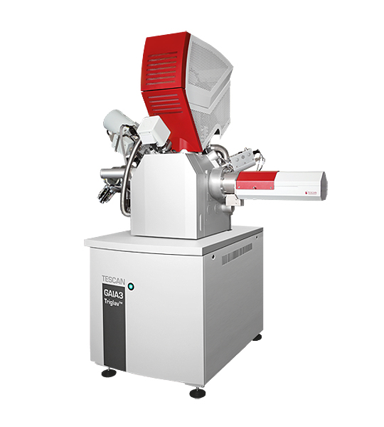
GAIA3
Extraordinary Ultra-High Resolution imaging and extremely precise nanoengineering.
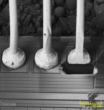
The preparation of high-quality ultra-thin TEM lamella, delayering processes in technology nodes, precise nanopatterning or high-resolution 3D reconstructions are just some of the applications in which GAIA3 excels.
PRODUCT BROCHURE

GAIA3 brochure
Extraordinary Ultra-High Resolution imaging and extremely precise nanoengineering. Download GAIA3 brochure!
PDF – 6.1 MB
KEY FEATURES
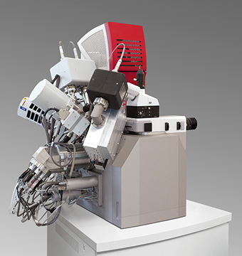
Triglav™ - newly designed UHR electron column
- TriLens™ - objective system: unique combination of three-lens objective and crossover-free beam path
- Advanced detection system with multiple SE and BSE detectors - TriSE™ and TriBE™
- Triglav™ - Ultimate ultra-high resolution at low beam energy: 1 nm at 1 keV and 0.7 nm at 15 keV
- Electron beam currents up to 400 nA and rapid beam energy changes
- Optimised column geometry for accommodating large wafers up to 8”
Specification
| Electron Optics | |
|---|---|
| Electron Gun | High brightness Schottky emitter |
| Resolution | |
| Standard mode In-Beam SE | 0.7nm at 15keV 1.4nm at 1keV 1.7nm at 500eV |
| Beam Deceleration Mode (Option) |
1.0nm at 1 keV - SE (BDM) |
| Magnification at 30keV | 4 x - 1,000,000 x |
| Probe Current | 2 pA to 400 nA |
Cobra FIB column
High-performance Ga FIB column for ultimate precision in nanoengineering.
- Probe current: 1 pA 50 nA
- Resolution: < 2.5 nm at 30 kV at SEM-FIB coincidence point
- Cobra guarantees the shortest time to result in cross-sectioning and TEM sample preparation
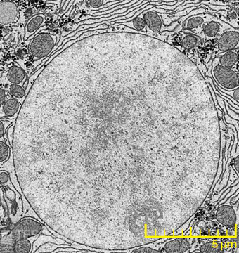
- Ideal for 3D ultra-structural studies of biological specimens such as tissue and whole cells
- Excellent performance at low kV ideal for polishing ultra-thin lamella and for reducing amorphous layers
Ion Optics
| Ion column | Cobra |
|---|---|
| Ion Gun | Ga LIMS |
| Resolution | <2.5 nm at 30Kev (at SEM-FIB coincidence point) |
| Probe current | 1 pA to 50nA |
| Accelerating Voltage | 0.5kV to 30kV |
| Magnification | Minimum 150 × at coincidence point and 10 kV (corresponding to 1 mm field of view), maximum 1,000,000 × |
| SEM-FIB coincidence at | WD 5 mm for SEM – WD 12 mm for FIB |
| SEM-FIB angle | 55° |
Application
Semiconductors & Microelectronics
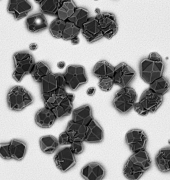
Material Science
Life Sciences
Earth Sciences
서울 금천구 가산동 서부샛길 606 대성디폴리스 A-802 (주)테스칸코리아
대표자 : 김재환 l 사업자등록번호 : 109-81-97174 l 개인정보책임자 : 정옥윤 l TEL : 02-861-8056 l FAX : 02-861-8066 l 이메일 : tescan@tescan.co.kr
Copyright ⓒ (주)테스칸코리아. ALL Rights Reserved. [[개인정보취급방침]]
대표자 : 김재환 l 사업자등록번호 : 109-81-97174 l 개인정보책임자 : 정옥윤 l TEL : 02-861-8056 l FAX : 02-861-8066 l 이메일 : tescan@tescan.co.kr
Copyright ⓒ (주)테스칸코리아. ALL Rights Reserved. [[개인정보취급방침]]

브로슈어 신청