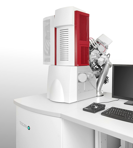
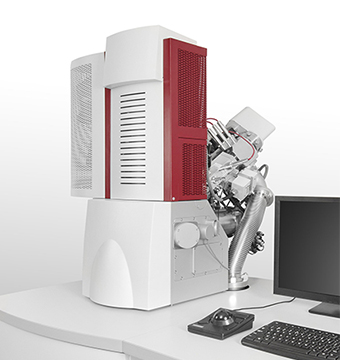
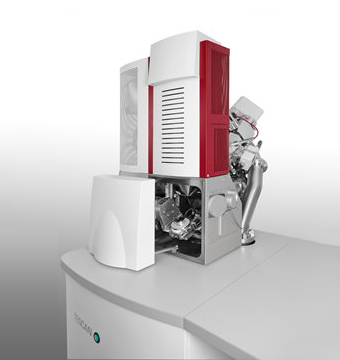
FERA3
The world’s first fully integrated Xe plasma source focused ion beam (FIB) with scanning electron microscopy (SEM) enables extremely high ion currents up to 2 μA which results in increased milling speeds that can be up to 50 times faster compared to conventional Ga source FIBs.
PRODUCT BROCHURE

FERA3 brochure
The world’s first fully integrated Xe plasma FIB-SEM. Download FERA3 brochure!
PDF – 6.1 MB
KEY FEATURES
- The unique Wide Field Optics™ design with a proprietary Intermediate Lens (IML) offers a variety of working and display modes with enhanced field of view or depth of focus
- Real time In-Flight Beam Tracing™ for performance and beam optimization. Also includes direct and continual control of beam parameters.
- Fully automated electron optics set-up and alignment
- Rapid imaging with rates up to 20 ns
Specification
| Electron Gun | High Brightness Schottky Emitter |
|---|---|
| Resolution | |
| SE | 1.2nm at 30keV / 1nm at 30keV (Optional In-Beam detector) 1.5nm at 3keV (Optional Beam Deceleration Mode) |
| BSE | 2.0nm at 30keV |
| Magnification | 2x - 1,000,000x (LM), 1x - 1,000,000x (XM/GM) |
| Accelerating Voltage | 200eV to 30keV / 50eV to 30kV with BDM option |
| Probe Current | 1pA to 200nA (Optional 1pA to 400nA) |
| Stage | 5-axis fully Compucentric stage |
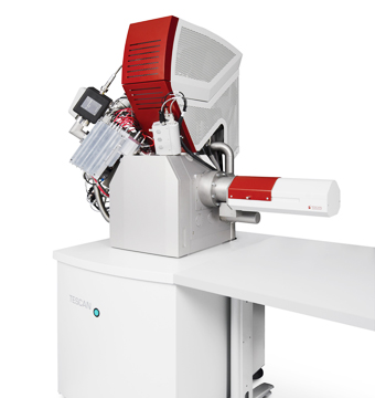
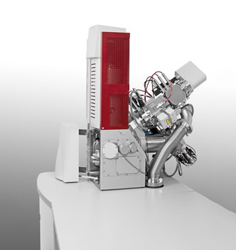
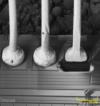
Extremely powerful Xe plasma FIB column
ECR-generated Xe plasma ion source FIB column for achieving the most challenging large-scale milling tasks in unbeatable short times frames
- 50x faster than Ga LMIS FIBs.
- Ion beam range current of 1 pA to 2 µA and resolution of < 25 nm
- Newly developed high resolution Xe plasma FIB column (Optional) achieving resolution of < 15 nm for extended patterning capabilities
- Large-mass xenon ions with larger FIB current range for ultra-fast sputtering even without gas-assisted enhancement
- Significant reduction in ion implantation compared to Ga LMIS FIBs
- Rocking Stage - An effective and optimised polishing strategy against curtaining effect
Ion Optics
| Ion column | HR i-FIB | i-FIB |
|---|---|---|
| Ion Gun | Xe plasma ion source | |
| Accelerating voltage | 3kV to 30kV | |
| Probe current | 1 pA to 1 µA | 1 pA to 2 µA |
| Resolution (at 30 keV) | < 15 nm | < 25 nm |
| Magnification | Minimum 150 × at coincidence point and 10 kV (corresponding to 1 mm field of view), maximum 1,000,000 × | |
| SEM-FIB coincidence at | WD 9 mm (FERA3) / WD 5 mm (XEIA3) for SEM – WD 12 mm for FIB | |
| SEM-FIB angle | 55° | |
Application
Semiconductors & Microelectronics
Material Science
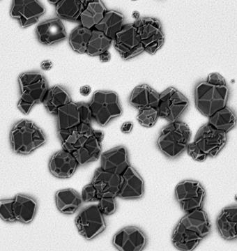
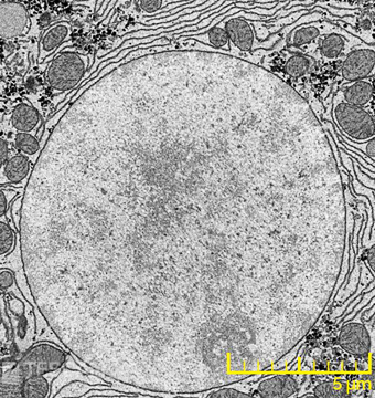
Life Sciences
Earth Sciences
서울 금천구 가산동 서부샛길 606 대성디폴리스 A-802 (주)테스칸코리아
대표자 : Pavel Sustek(파벨수스텍) l 사업자등록번호 : 109-81-97174 l 개인정보책임자 : 정옥윤 l TEL : 02-861-8056 l FAX : 02-861-8066 l 이메일 : tescan@tescan.co.kr
Copyright ⓒ (주)테스칸코리아. ALL Rights Reserved. [[개인정보취급방침]]
대표자 : Pavel Sustek(파벨수스텍) l 사업자등록번호 : 109-81-97174 l 개인정보책임자 : 정옥윤 l TEL : 02-861-8056 l FAX : 02-861-8066 l 이메일 : tescan@tescan.co.kr
Copyright ⓒ (주)테스칸코리아. ALL Rights Reserved. [[개인정보취급방침]]

브로슈어 신청