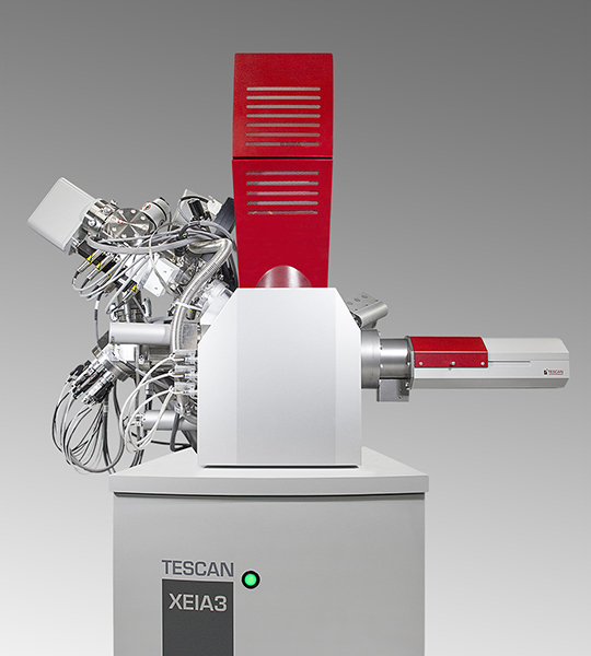
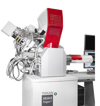
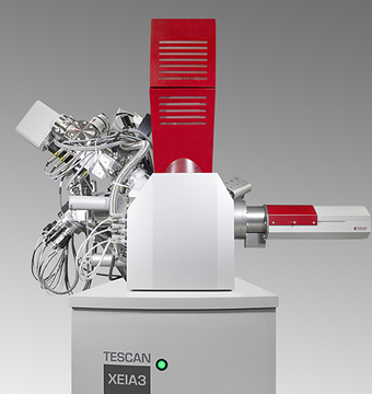
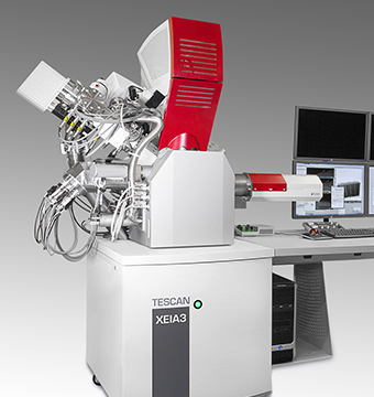
XEIA3
Extraordinary Ultra-High Resolution imaging and extremely powerful Xe plasma ion source FIB column
PRODUCT BROCHURE

XEIA3 brochure
Extraordinary ultra-high resolution imaging and extremely fast micromachining. Download XEIA3 brochure!
PDF – 6.1 MB
KEY FEATURES
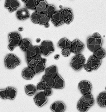
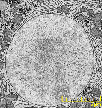
Triglav™ - newly designed UHR electron column
- TriLens™ - objective system: unique combination of three-lens objective and crossover-free beam path
- Advanced detection system with multiple SE and BSE detectors - TriSE™ and TriBE™
- Triglav™ - Ultimate ultra-high resolution at low beam energy: 1 nm at 1 keV and 0.7 nm at 15 keV
- Electron beam currents up to 400 nA and rapid beam energy changes
- Optimised column geometry for accommodating large wafers up to 8” and 12”
Specification
| Electron Optics | |
|---|---|
| Electron Gun | High brightness Schottky emitter |
| Resolution | |
| Standard mode In-Beam SE | 0.7nmat15keV 1.4nmat1keV |
| Beam Deceleration Mode (Option) |
1.0nm at 1 keV - SE (BDM) |
| Magnification at 30keV | 4 x - 1,000,000 x |
| Probe Current | 2 pA to 400 nA |
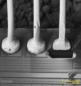
Extremely powerful Xe plasma FIB column
Xe plasma ion source FIB column for achieving the most challenging large-scale milling tasks in unbeatable short times frames
- 50x faster than Ga LMIS FIBs.
- Ion beam range current of 1 pA to 2 µA and resolution of < 25 nm
- Newly developed high resolution Xe plasma FIB column (Optional) achieving resolution of < 15 nm for extended patterning capabilities
- Large-mass xenon ions with larger FIB current range for ultra-fast sputtering even without gas-assisted enhancement
- Significant reduction in ion implantation compared to Ga LMIS FIBs
- Rocking Stage - An effective and optimised polishing strategy against curtaining effect
Ion Optics
| Ion column | HR i-FIB | i-FIB |
|---|---|---|
| Ion Gun | Xe plasma ion source | |
| Accelerating voltage | 3kV to 30kV | |
| Probe current | 1 pA to 1 µA | 1 pA to 2 µA |
| Resolution (at 30 keV) | < 15 nm | < 25 nm |
| Magnification | Minimum 150 × at coincidence point and 10 kV (corresponding to 1 mm field of view), maximum 1,000,000 × | |
| SEM-FIB coincidence at | WD 9 mm (FERA3) / WD 5 mm (XEIA3) for SEM – WD 12 mm for FIB | |
| SEM-FIB angle | 55° | |
Application
Semiconductors & Microelectronics
Material Science
Life Sciences
Earth Sciences
서울특별시 강서구 마곡중앙로 143, 비동 2층 4호, 5호, 6호(마곡동, 르웨스트 시티) (주)테스칸코리아
대표자 : Pavel Sustek(파벨수스텍) l 사업자등록번호 : 109-81-97174 l 개인정보책임자 : Pavel Sustek(파벨수스텍)
TEL : 02-2261-6650 l FAX : 02-2261-6654 l 이메일 : invoicing-tk@tescan.com
Copyright ⓒ (주)테스칸코리아. ALL Rights Reserved. [[개인정보취급방침]]
대표자 : Pavel Sustek(파벨수스텍) l 사업자등록번호 : 109-81-97174 l 개인정보책임자 : Pavel Sustek(파벨수스텍)
TEL : 02-2261-6650 l FAX : 02-2261-6654 l 이메일 : invoicing-tk@tescan.com
Copyright ⓒ (주)테스칸코리아. ALL Rights Reserved. [[개인정보취급방침]]

브로슈어 신청